case 03 · Personal · 2024 – 2025
8-bit breadboard computer
A Turing-complete 8-bit CPU wired up from discrete logic chips on breadboards — ALU, registers, RAM, clock, control unit. Custom assembly language for programming it.
What it is
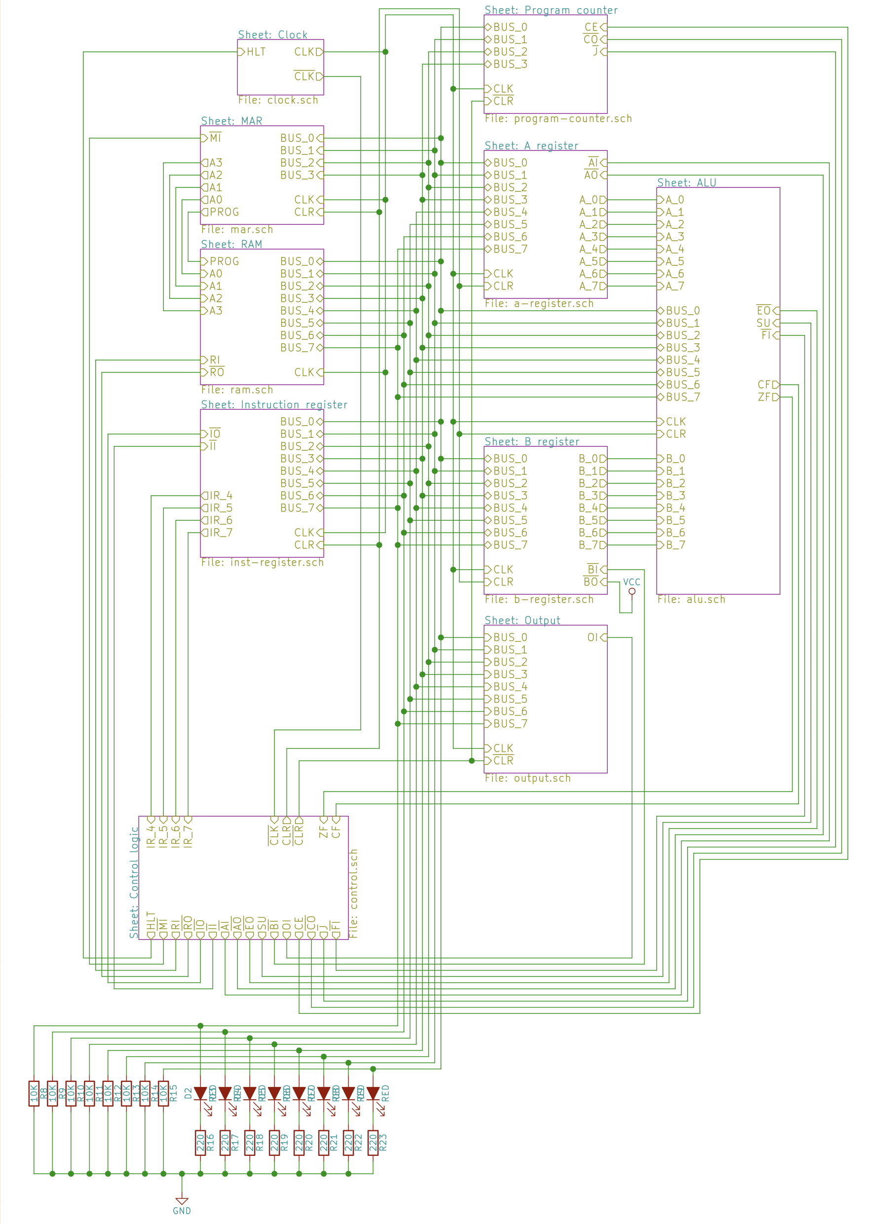
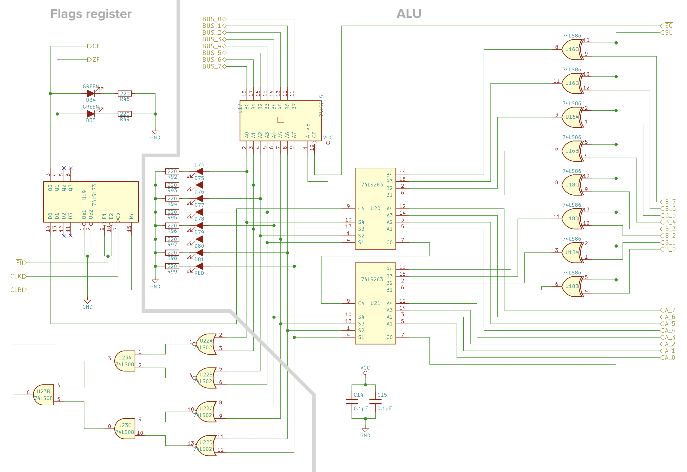
A working 8-bit computer built entirely from 7400-series logic and a few 74181-style ALU chips on breadboards — no microcontroller, no FPGA, no shortcuts. The CPU has a real ALU, an 8-bit register file, a RAM module, a clock module, and a microcoded control unit that decodes a small instruction set.
What I built
- An ALU capable of add/subtract and bitwise ops on 8-bit operands.
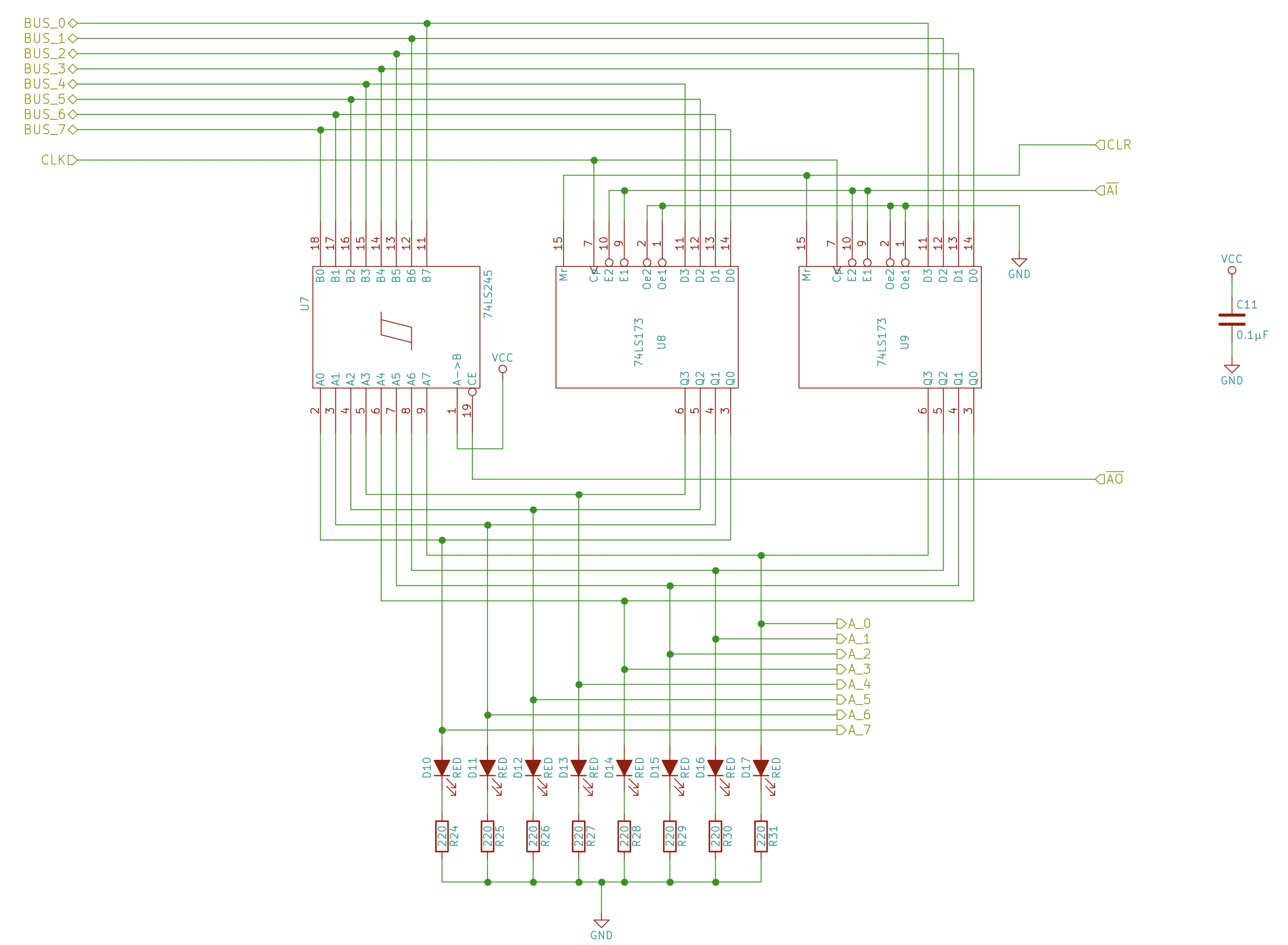
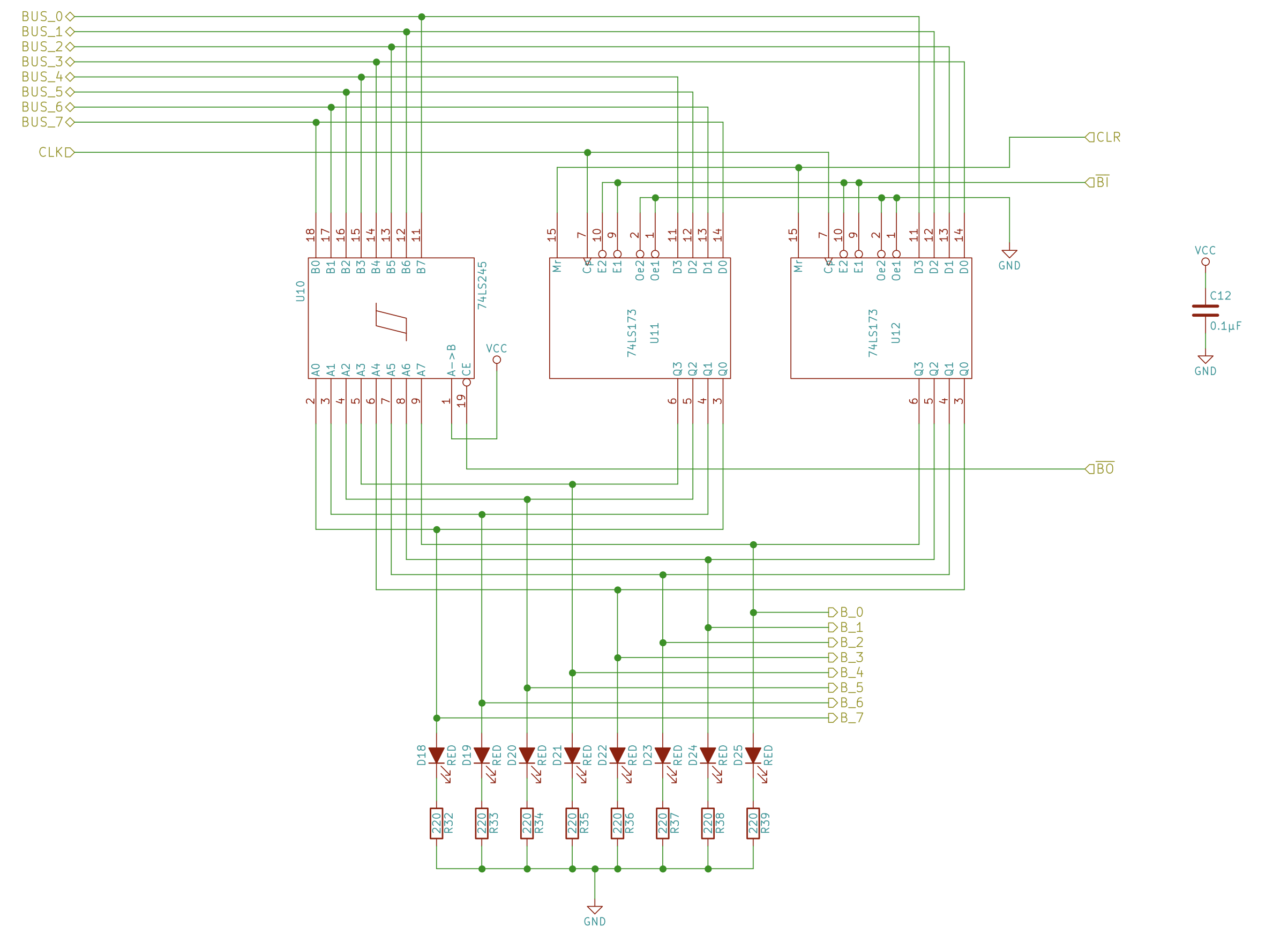
- An 8-bit register file built from D-flip-flops with tristate outputs onto the shared bus.
- A RAM module with address-latched reads/writes.
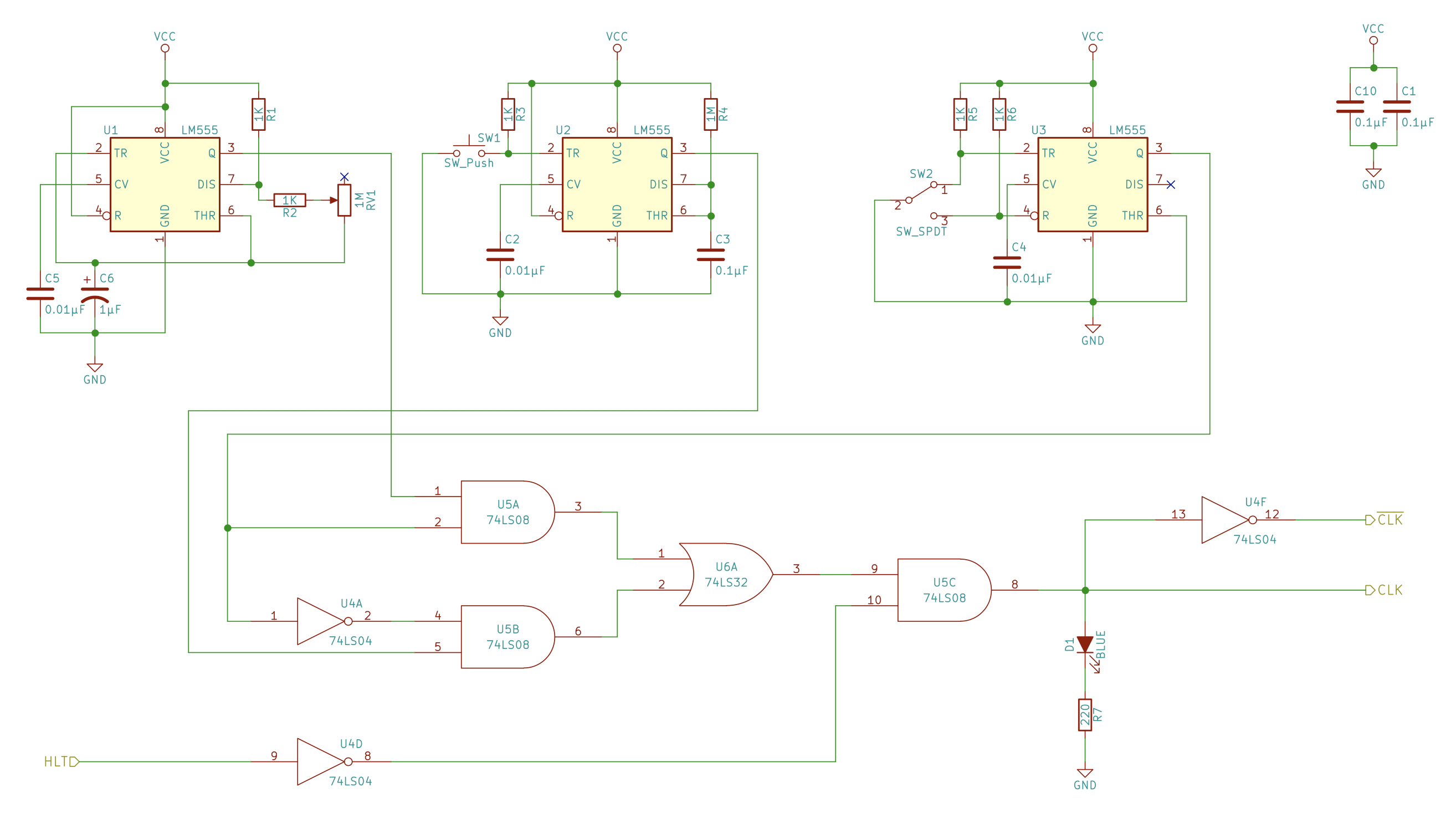
- A clock module with adjustable frequency and single-step debugging.
- A control unit that drives the right enable/load lines for each instruction in the ISA.
The instruction set
I designed a small custom ISA tailored to the hardware — load, store, add, sub, jump, conditional branch, halt — and wrote a hand-assembler so programs could be written in mnemonics and burned into the RAM. Turing-completeness comes from the combination of conditional branching, memory writes, and unbounded program length.
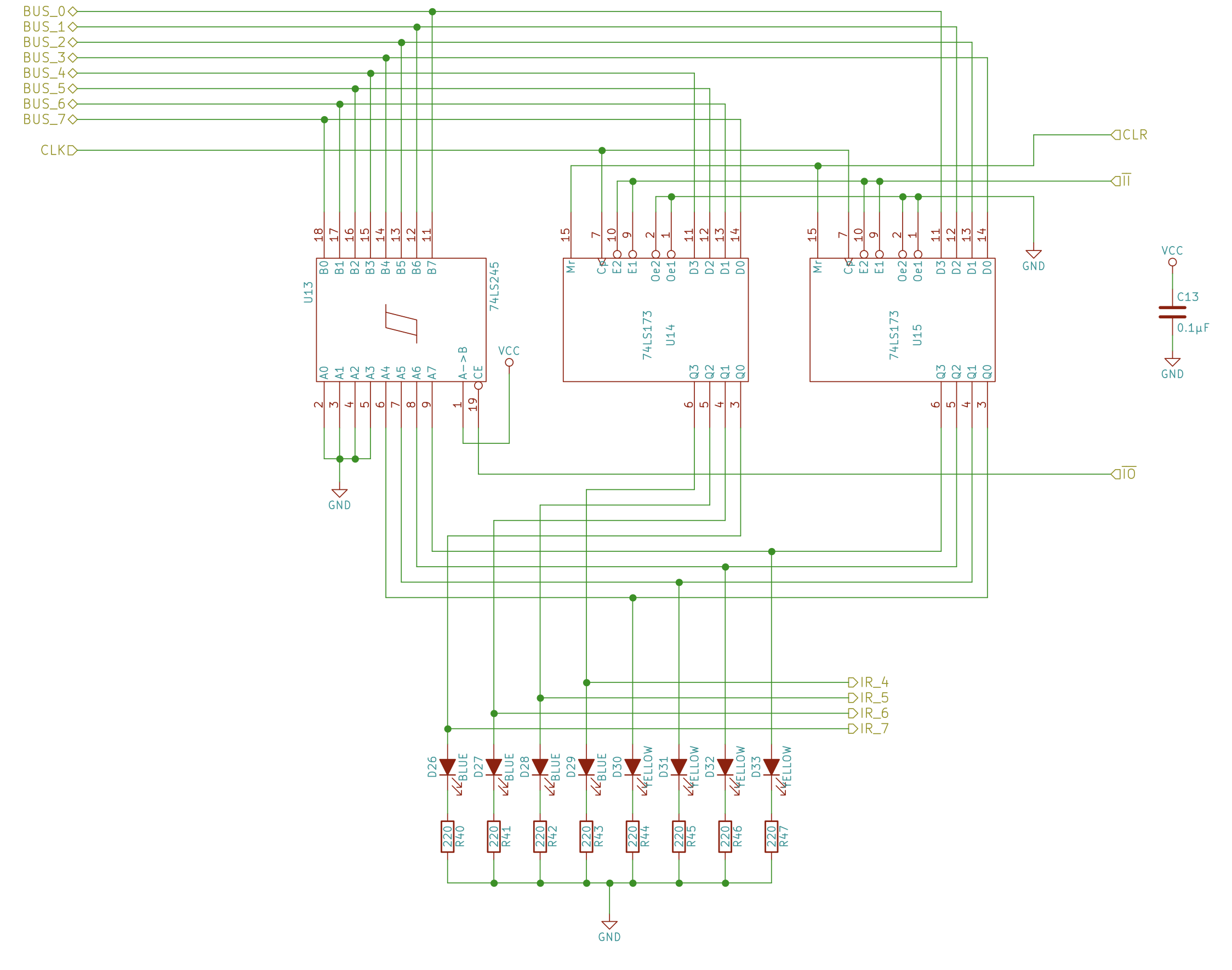
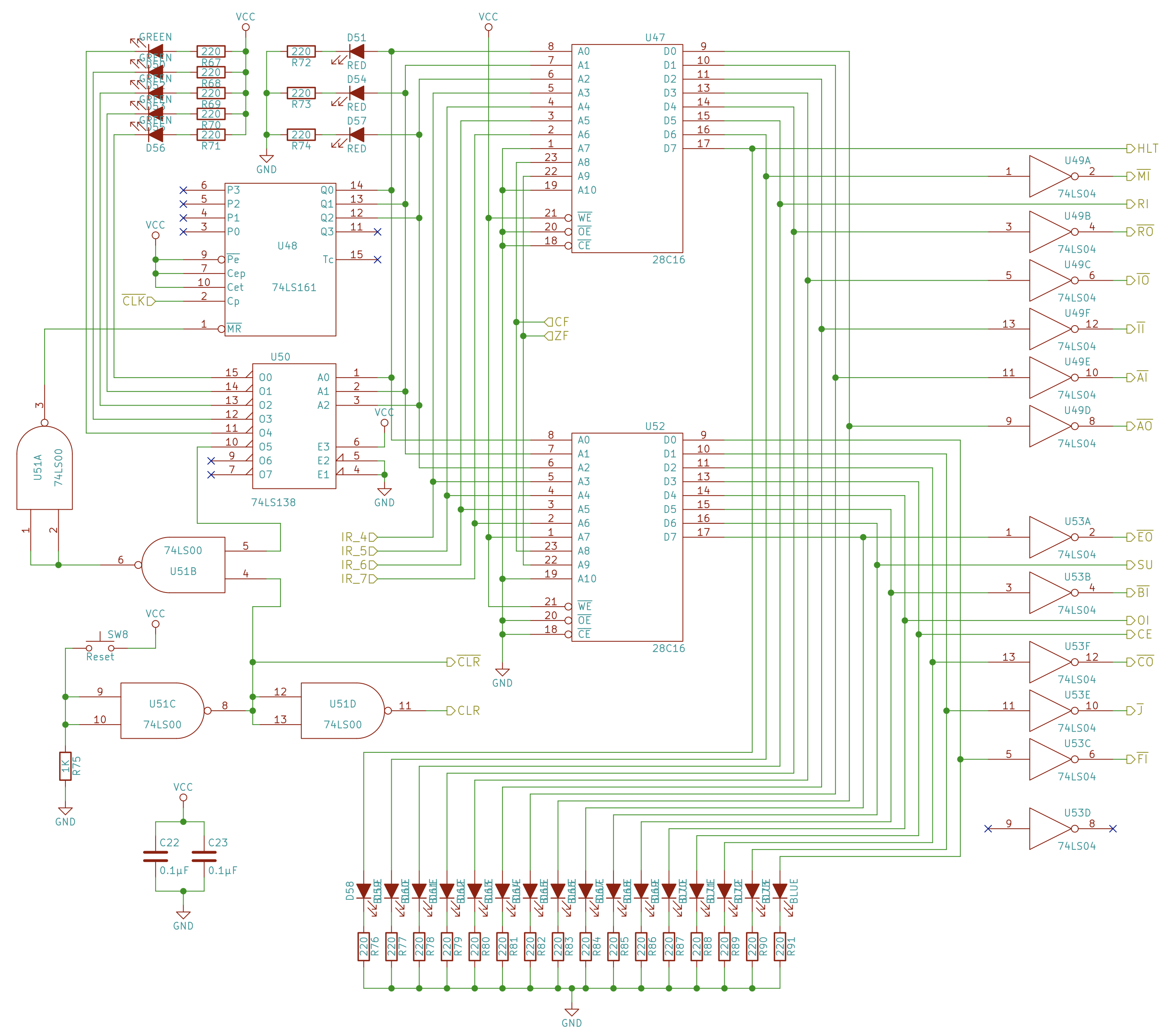
(opcode, step) into the bitmap of enable/load lines that drive each micro-op. Schematic from eater.net.Why do it
Software engineers usually treat the CPU as a black box. Building one from gates makes everything below the C abstraction concrete: what an instruction is, what a register is, how a clock advances state. Every higher-level decision later — pipelines, cache coherence, memory ordering — makes sense once you've seen the gates underneath.
Parts list
Bill of materials — drawn from Ben Eater's published list at eater.net/8bit/parts. Quantities only; prices omitted.
Breadboards & wiring
- 14×Breadboard
- 1×22 AWG solid tinned-copper hook-up wire
Resistors
- 10×1 kΩ resistor
- 9×10 kΩ resistor
- 1×100 kΩ resistor
- 24×470 Ω resistor
- 1×1 MΩ resistor
- 1×1 MΩ potentiometer
Capacitors
- 6×0.01 µF capacitor
- 16×0.1 µF capacitor
- 1×1 µF capacitor
Clock module
- 4×555 timer IC
Logic gates & basic ICs
- 2×74LS00 — quad NAND
- 1×74LS02 — quad NOR
- 5×74LS04 — hex inverter
- 3×74LS08 — quad AND
- 1×74LS32 — quad OR
- 2×74LS86 — quad XOR
Registers & counters
- 1×74LS107 — dual JK flip-flop
- 8×74LS173 — 4-bit D register
- 1×74LS273 — octal D flip-flop
- 2×74LS161 — 4-bit binary counter
Multiplexers & decoders
- 1×74LS138 — 3-to-8 decoder
- 1×74LS139 — dual 2-to-4 decoder
- 4×74LS157 — quad 2-to-1 mux
ALU & memory
- 2×74LS283 — 4-bit binary adder
- 2×74189 — 64-bit RAM
Bus & control
- 6×74LS245 — octal bus transceiver
- 3×28C16 EEPROM
Input / output
- 3×Double-throw toggle switch
- 3×Momentary 6 mm tact switch
- 1×8-position DIP switch
- 1×4-position DIP switch
- 44×Red LED
- 8×Yellow LED
- 12×Green LED
- 21×Blue LED
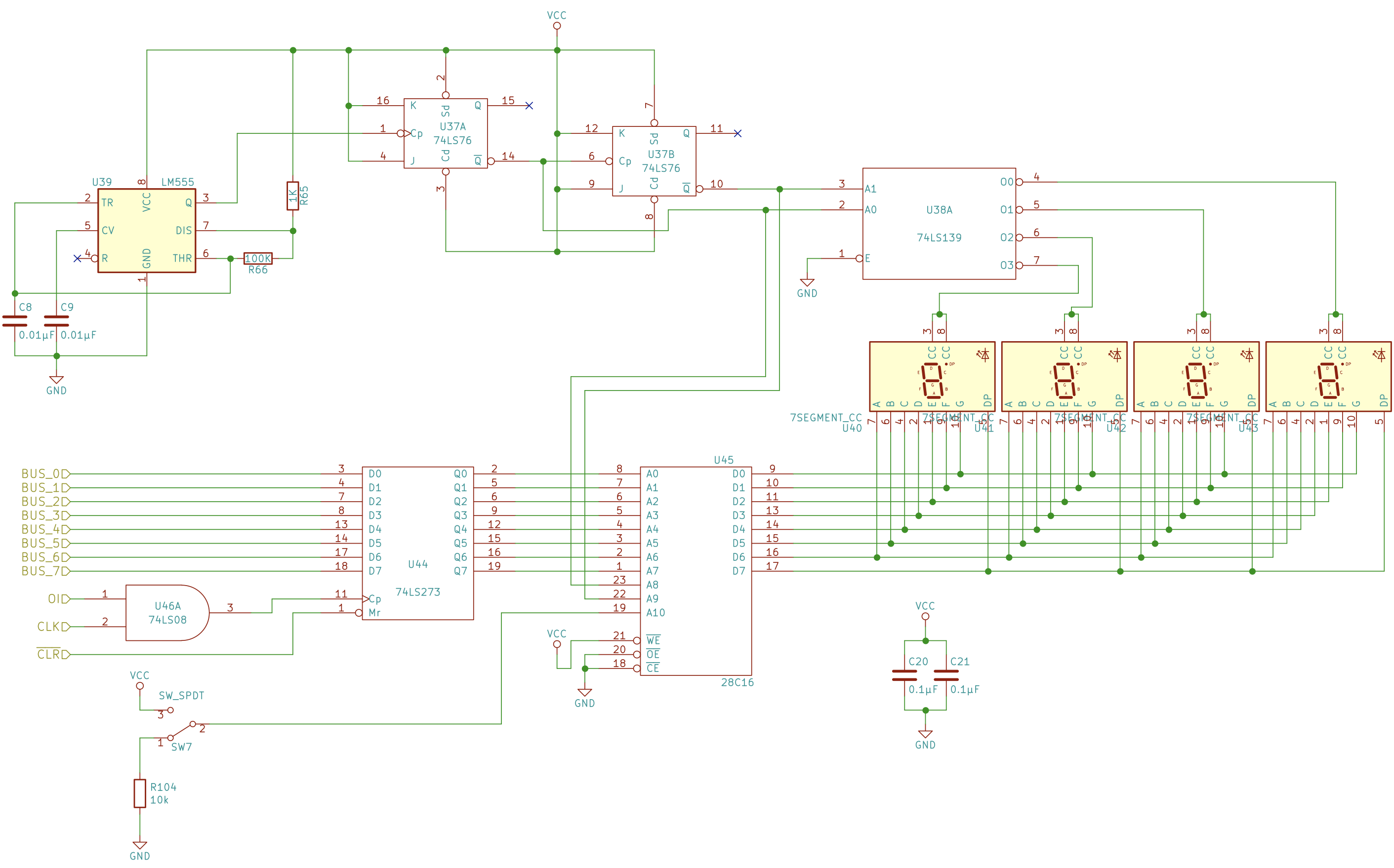
- 4×Common-cathode 7-segment display
EEPROM programmer
- 1×Arduino Nano
- 2×74HC595 — shift register
- Word size
- 8-bit
- Logic
- Discrete 7400-series chips
- Memory
- RAM module + microcoded control ROM
- Programmability
- Custom ISA + hand-assembler
What's next
- Stack & subroutines — add a stack pointer register and CALL/RET instructions so programs can use functions; requires one more register and two new microcode sequences
- Expand RAM — the current design has 16 bytes of addressable RAM; routing more address lines to the RAM chip would get to 256 bytes and make real programs possible
- Assembler — replace hand-assembly with a simple Python assembler that takes a text file of mnemonics and outputs the binary to load
- Serial output — add a 74HC595 shift register or a UART chip so the computer can write text to a terminal rather than just the 7-segment display
- PCB — translate the breadboard layout to a proper PCB; cleaner signals, no loose wires, and a far more reliable machine